 |
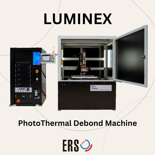
MUNICH, March 13, 2024 /PRNewswire/ -- ERS electronic, the industry leader of thermal management solutions for semiconductor manufacturing is presenting the first machine from its innovative Luminex product line featuring the cutting-edge "PhotoThermal" debonding technology for wafer and panels up to 600 x 600 mm.

PhotoThermal debonding is a zero stress debonding method that uses a highly controlled flash lamp to separate the carrier from the substrate. A key component of the PhotoThermal debonding process is the glass carrier with light absorbing layer (CLAL) that converts light energy from the lamp to thermal energy, enabling a smooth separation. Thanks to the CLAL, additional adhesive release layer coating together with the bond layer is not needed, thereby reducing process steps and the associated complexity and operations cost, saving users up to 30% in cost of ownership compared to traditional laser debonding.
ERS's semi-automatic machine is the first in a series of machines belonging to the Luminex product line. ERS is in the advanced stages of developing its fully automatic counterpart for 300 mm wafers, which will be released before end of Q2. As part of the comprehensive product line, the company will offer the automatic machine with several modular add-ons, further enhancing product quality and yield.
"PhotoThermal debonding represents a significant leap forward in semiconductor manufacturing," says Debbie-Claire Sanchez, Vice President and Head of the APEqS Business Unit at ERS. "The first machine in our Luminex line is a great springboard for research and development teams who are working on Advanced Packaging developments or New Product Introduction, and we invite companies to send us their samples for testing."
Starting from April, the semi-automatic machine will be deployed in ERS's lab in Shanghai, China, and in Germany, where it will be used to test customer wafer and panel samples and be available for demonstrations.
About ERS:
ERS electronic GmbH, based in the Munich suburb of Germering, has been providing innovative thermal management solutions to the semiconductor industry for more than 50 years. The company has gained an outstanding reputation, notably with its fast and accurate air cooling-based thermal chuck systems for test temperatures ranging from -65 °C to +550 °C for analytical, parameter-related and manufacturing probing. In 2008, ERS extended its expertise to the Advanced Packaging market. Today, their fully automatic and manual debonding and warpage adjust systems can be found on the production floors of most semiconductor manufacturers and OSATs worldwide. The company has received widespread recognition in the industry for their ability to tackle complex warpage issues that arise in the Fan-out wafer-level packaging manufacturing process.