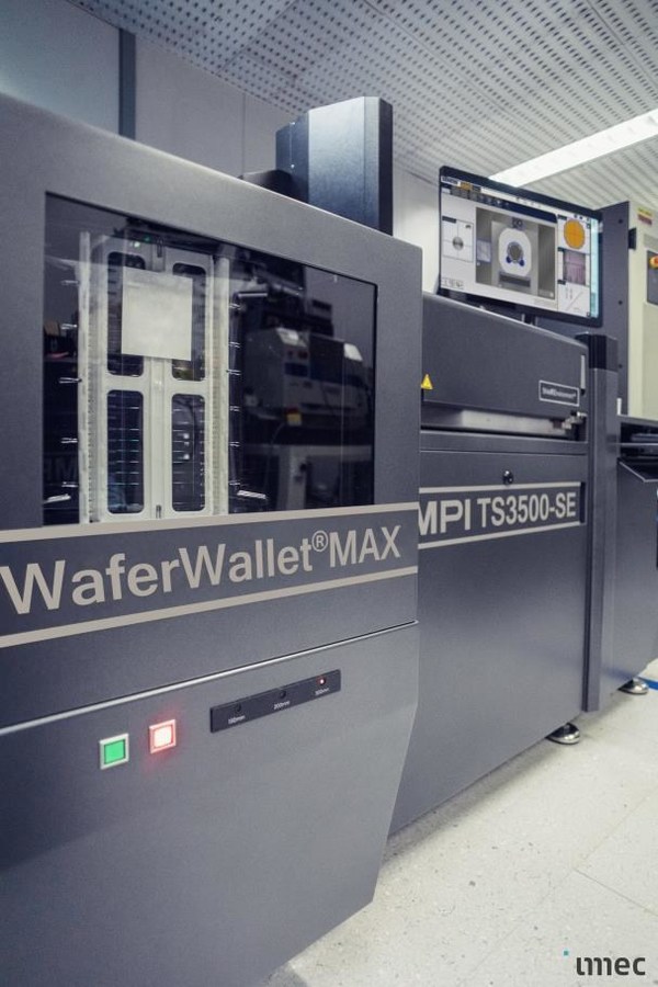
HSINCHU, July 29, 2022 /PRNewswire/ -- MPI Corporation's Advanced Semiconductor Test Division, an industry and innovation leader of semiconductor test solutions initiated the integration of the TS3500-SE automated wafer probe test system with WaferWallet®MAX, a multi-purpose cassette, FOUP self-docking 200 mm and 300 mm handling solution, into a leading WLR test process.

MPI Corporation has Installed its WaferWallet®MAX for 200mm and 300mm WLR Processes MPI Corporation’s Advanced Semiconductor Test Division, an industry and innovation leader of semiconductor test solutions initiated the integration of the TS3500-SE automated wafer probe test system with WaferWallet®MAX, a multi-purpose cassette, FOUP self-docking 200 mm and 300 mm handling solution, into a leading WLR test process.
The WaferWallet®MAX provides an automation solution by increasing overall testing time over 400% without compromising measurement accuracy and capability. It increases testing efficiency and productivity further by reducing temperature soaking time (part of the overall test time), while enabling hot/cold wafer swapping – which is a unique capability of loading and unloading wafers while the chuck remains at any test temperature.
MPI successfully collaborates with imec for integration of its WaferWallet®MAX solution in imec's Advanced Reliability Robustness and Test (AR²T) department, leveraging their 200 and 300mm WLR qualification activities in support of their Logic, Insite and Memory R&D programs.
"Significantly increasing the throughput and obtaining more statistical data leads to faster time to market for our customer," said Stojan Kanev, General Manager of the Advanced Semiconductor Test Division. "In addition, the unsurpassed flexibility and field-upgradability without adding extra cost, the WaferWallet®MAX 300MM is a natural extension to MPI's automated TS3500 Series of wafer test systems, providing a cost-effective automation solution, for increasing test cell efficiency and lowering the overall cost of test."
WaferWallet®MAX seamlessly integrates automated cassette scanning, wafer pre-alignment, top and bottom ID reading via MPI's SENTIO® multi touch prober control software suite. SENTIO® remains the undisputed market leader of intuitive operation and customer centric approach while offering unique, free upgrade path and public domain programmable tools.
About MPI Corporation
Founded in 1995 and headquartered in Hsinchu, Taiwan, MPI Corporation is a global technology leader in Semiconductor, Light Emitting Diode (LED), Photo Detectors, Lasers, Materials Research, Aerospace, Automotive, Fiber Optic, Electronic Components and more. MPI's four main business sectors include Probe Card, Photonics Automation, Advanced Semiconductor Test and Thermal Divisions. MPI products range from various advanced probe card technologies, probers, testers, material handlers, inspection and thermal air systems. Many of these products are accompanied by state-of-the-art Calibration and Test & Measurement software suites. The diversification of product portfolio and industries allows a healthy environment for employee growth and retention. Cross pollination of product technologies allows each new innovation to provide differentiation in areas that are meaningful to our precious customer base.
For more information please visit: mpi-corporation.com