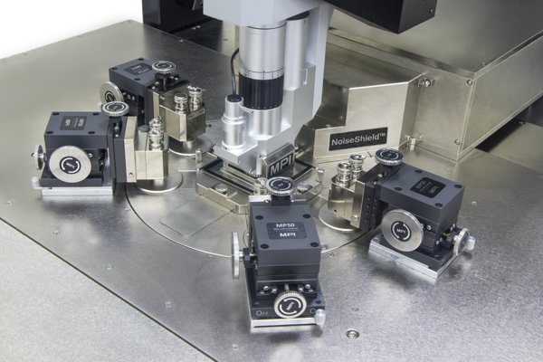
HSINCHU, Nov. 6, 2019 /PRNewswire/ -- MPI introduced a new NoiseShield™ option, which provides excellent EMI-shielding, low impedance grounding and shortest possible cable lengths to reduce parasitic capacitance and to maximize the test system roll-off frequency. It reduces external magnetic field influences on the measurement results and makes the 1/f, RTN setup more robust and test lab location less-independent. It makes the probe station completely "invisible" and enables the measurement results down to the physical limit of the test instrumentation.

"The MPI NoiseShield™ is the next step in providing a high value solution for 1/f measurements." Said Toe Naing Swe, Director Device Modeling, at MPI Advanced Semiconductor Test Division. "In combination with the MPI ShielDEnvironment™, users can now experience excellent EMI-Shielding for not only device under test (DUT) and the measurement instrument (such as pre-amplifier unit of ProPlus 9812DX), it also includes all cables and connectors. The fully integrated solution also shortens the cables by placing the LNA very close to DUT. Installed on TS3500-SE with MPI WaferWallet®, customers can now perform, for the first time ever, unsurpassed fully-automated 1/f measurements. MPI SENTIO® Software Suite includes native drivers for the ProPlus Design Solutions product suite, such as BSIMProPlus™ and NoiseProPlus™, making such automation out of the box easy."
"The MPI prober is excellent and best I have ever worked with", said Dr. Zhihong Liu, CEO and Co-Founder of ProPlus Design Solutions Inc. "For noise measurement, it gives the best performance both in shielding and reduction in parasitics. With it, we are able to reach the limit of our system without trade-offs. Using the High Precision LNA in 9812DX, we can get to the floor noise of 3e-27 A^2/Hz with >20KHz bandwidth and accurately monitor the bias current down to pA level simultaneously. It can also measure down to 0.1Hz in the low frequency end without the introduction of mechanical vibration. Using the MPI prober, we also measured a MOSFET with 10MHz on-wafer bandwidth and the noise level is reaching to our Wideband LNA noise floor."
About MPI Corporation
Founded in 1995 and headquartered in Hsinchu, Taiwan, MPI Corporation is a global technology leader in Semiconductor, Light Emitting Diode (LED), Photo Detectors, Lasers, Materials Research, Aerospace, Automotive, Fiber Optic, Electronic Components and more. MPI's four main business sectors include Probe Card, Photonics Automation, Advanced Semiconductor Test and Thermal Divisions. MPI products range from various advanced probe card technologies, probers, testers, material handlers, inspection and thermal air systems. Many of these products are accompanied by state-of-the-art Calibration and Test & Measurement software suites. The diversification of product portfolio and industries allows a healthy environment for employee growth and retention. Cross pollination of divisional product technologies stimulates MPI product innovations that are meaningful to our precious customer base.
For more information please visit: www.mpi-corporation.com
About ProPlus Design Solutions
ProPlus Design Solutions, Inc. delivers Electronic Design Automation (EDA) solutions with the mission to enhance the link between design and manufacturing. As the leading provider of nano-scale SPICE modeling, the innovative giga-scale SPICE simulation and design for yield (DFY) applications, it provides the industry's golden SPICE modeling platform, the first and only GigaSpice simulator, and the only integrated DFY design platform. Founded in 2006, ProPlus Design Solutions has R&D centers in the San Jose, Beijing, Jinan, and offices in Tokyo, Hsinchu, and Shanghai.
For more information, please visit: www.proplussolutions.com
Photo - https://photos.prnasia.com/prnh/20191101/2629470-1?lang=0