KAOHSIUNG, Nov. 3, 2023 /PRNewswire/ -- Silicon Carbide (SiC) is pivotal in semiconductors, with E&R Technology committed to boosting process yields via vital SiC integration solutions. SiC surpasses silicon with high-temperature resilience, superior voltage tolerance, potent power capabilities, and minimal losses, making it ideal for automotive and 5G industries.

E&R SiC Solution
While SiC wafers mainly come in 4-inch and 6-inch sizes, efforts are ongoing to develop 8-inch and 12-inch wafers, despite process yield challenges. Tier 1 IDM manufacturers like ONSEMI, Infineon, and Bosch are announcing expansion and product plans for 2024-2025.
E&R collaborates with global industry leaders and suppliers, offering key SiC integration solutions:
Laser Annealing: E&R deploys ultra-short wavelength lasers with their self-developed accelerated optics solution (ACES) for precise and uniform shallow annealing.
Wafer ID Marking: With over 30 years of laser expertise, E&R employs a 355nm UV laser, designed for SiC, meeting precision and throughput demands. It works for 6-inch, 8-inch, and 12-inch wafers, both topside and backside.
Wafer Dicing and Grooving: E&R uses industry-leading Pico second and Femto second laser technologies for cutting and grooving, achieving a minimum cut width of 3um. Combined with mechanical breaking technology, their machines achieve an accuracy of ±1um, and successfully reduce wafer chipping and cracking while minimizing the heat-affected zone (HAZ) with recast thickness below 2um.
Raman Spectroscopy: In collaboration with world-leading wafer foundries, E&R introduces Raman spectroscopy technology. By illuminating wafers with laser light on their surface or within, they induce Raman scattering, allowing effective waveform analysis to obtain fundamental information about wafers like internal stress, lattice structure, cracks, and element concentrations. This technology enables customers to comprehensively assess and adjust process parameters, reducing losses due to various defects, ultimately improving process yield.
Plasma Treatment: E&R provides various plasma treatment technologies, including LF, RF, and microwave plasma sources. These ensure a highly uniform cleaning process for wafers before wire bonding and molding, resulting in high surface hydrophilicity and a water contact angle of less than 10 degrees. Additionally, E&R proposes a plasma decarbonization solution to reduce carbon layers, thereby strengthening the subsequent backside metallization process.
E&R will continue to collaborate with customers and explore possibilities to achieve more efficient manufacturing processes, contributing to the future development of the semiconductor industry.
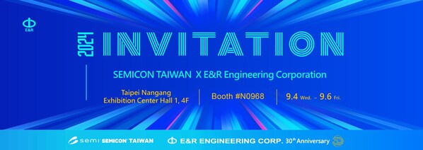
During Nov.14th-17th, E&R will exhibit in Semicon Europa at Messe München. Please stop by Booth# B2378 to have fruitful discussion with E&R.
E&R Website: https://en.enr.com.tw/